optostar
©2021 Optostar Ltd. All Rights Reserved
Since 2004
For Optics, Semiconductors, MEMS and Biochemical reserachers

OPTOSTAR Ltd.
Crystal Wafers with Micro and Nano process

Fabrication and sales for clean-room packed epi-ready polished sapphire wafer, in lots of 10.
Wafers are single-side polished at epi-ready grade and having good TTV.
c-plane 2-inch sapphire wafer
single-side polished
"Epitaxy-ready grade"
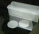

C-plane sapphire wafers
SEMI-compliant

2-inch c-plane sapphire wafers, packed 10 per container /Standard spec.

Wafer Material High-purity synthetic single-crystal sapphire
Wafer Diameter 2 inches (50.8mm +/-0.05mm)
Wafer Thickness 330um (+/-25um)
Orientation c-plane ( 0.2 +/- 0.1 degree) Off angle for epitaxy growth
Primary flat 16mm (+/-1.0mm)
Surface Front side: Polished at epitaxy-ready grade/ Back side: Lapped
Roughness,etc Ra <=0.5nm, TTV<=10um
Packing 10 pieces packed in a plastic container
Delivery About 7 days, Sent from Tokyo, Japan via FedEx
Payment By bank transfer in US dollars and Euros

inquiry Request a quote

inquiry
Home (Fused-silica wafers, sapphire wafers, and other crystal or glass wafers)
home
company
sapphire wafer
silicon
fused silica wafer
Easy-to-use epi-ready sapphire wafers for your R&D activities
SiC&ZnO
Substrates (Wafersj Tubes & Rods Windows & Lenses Polish & Thin Films LASER process